- 您现在的位置:买卖IC网 > Sheet目录2006 > LTC2446IUHF#TRPBF (Linear Technology)IC ADC 24BIT 8CH HI SPEED 38QFN
LTC2446/LTC2447
15
24467fa
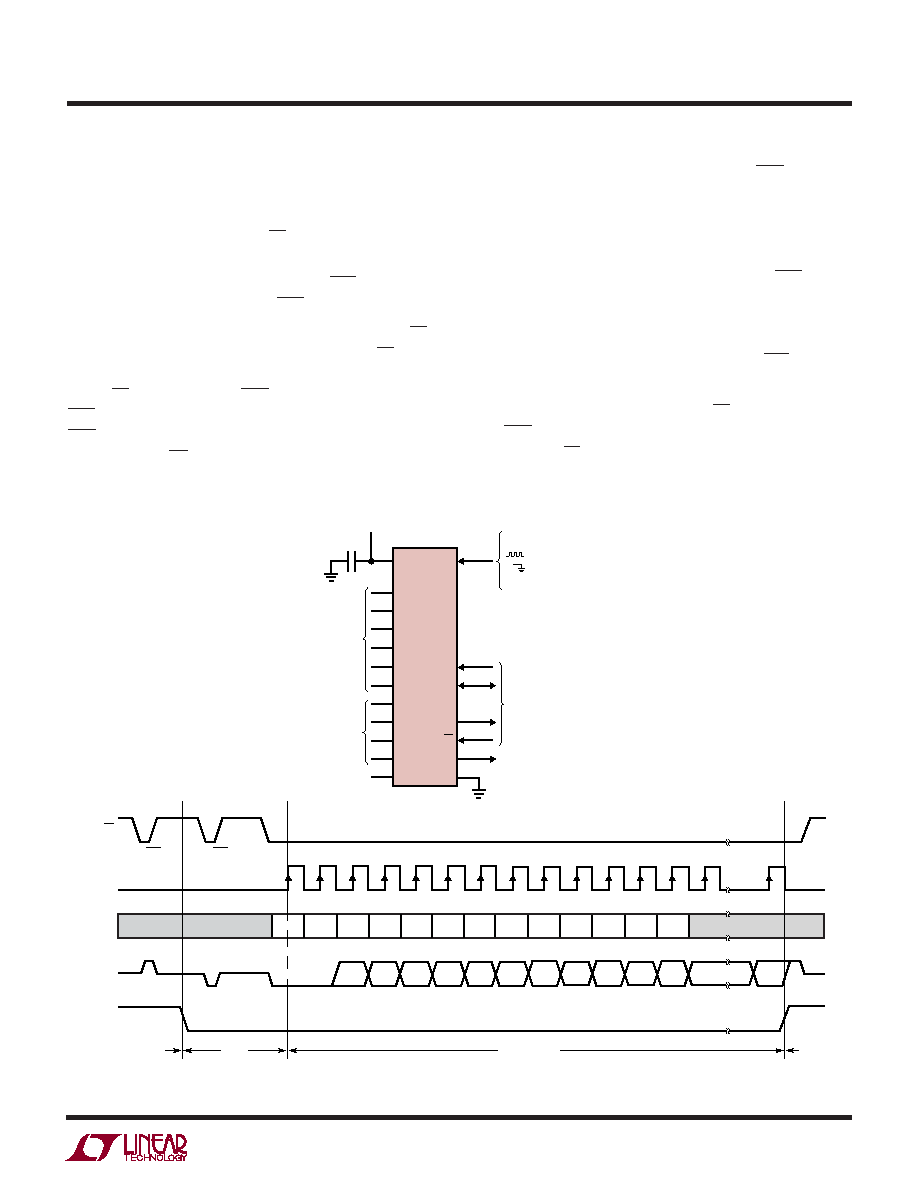
External Serial Clock, Single Cycle Operation
(SPI/MICROWIRE Compatible)
This timing mode uses an external serial clock to shift out
the conversion result and a CS signal to monitor and
control the state of the conversion cycle, see Figure 4.
The serial clock mode is selected by the EXT pin. To select
the external serial clock mode, EXT must be tied low.
The serial data output pin (SDO) is Hi-Z as long as CS is
HIGH. At any time during the conversion cycle, CS may be
pulled LOW in order to monitor the state of the converter.
While CS is pulled LOW, EOC is output to the SDO pin.
EOC = 1 (BUSY = 1) while a conversion is in progress and
EOC = 0 (BUSY = 0) if the device is in the sleep state.
Independent of CS, the device automatically enters the low
power sleep state once the conversion is complete.
When the device is in the sleep state (EOC = 0), its
conversion result is held in an internal static shift regis-
ter. The device remains in the sleep state until the first
rising edge of SCK is seen. Data is shifted out the SDO pin
on each falling edge of SCK. This enables external circuitry
to latch the output on the rising edge of SCK. EOC can be
latched on the first rising edge of SCK and the last bit of
the conversion result can be latched on the 32nd rising
edge of SCK. On the 32nd falling edge of SCK, the device
begins a new conversion. SDO goes HIGH (EOC = 1) and
BUSY goes HIGH indicating a conversion is in progress.
At the conclusion of the data cycle, CS may remain LOW
and EOC monitored as an end-of-conversion interrupt.
Alternatively, CS may be driven HIGH setting SDO to Hi-Z
and BUSY monitored for the completion of a conversion.
Figure 4. External Serial Clock, Single Cycle Operation
APPLICATIO S I FOR ATIO
WU
UU
MSB
BIT 28 BIT 27 BIT 26 BIT 25 BIT 24 BIT 23 BIT 22 BIT 21
BIT 20 BIT 19
BIT 0
LSB
Hi-Z
24467 F04
SIG
BIT 29
“0”
BIT 30
EOC
Hi-Z
CS
SCK
(EXTERNAL)
SDI
SDO
BUSY
BIT 31
1
0
EN
SGL
GLBL
A1
A0
OSR3
OSR2
OSR1
OSR0
TWOX
ODD
12345
6
7
89
10
11
12
13
14
32
CONVERSION
SLEEP
DATA OUTPUT
CONVERSION
TEST EOC
VCC
FO
REF67+
REF67–
CH0
CH1
CH2
CH7
COM
REFG+
REFG–
REF01+
REF01–
SCK
SDI
SDO
CS
GND
28
29
30
11
10
35
24
23
8
9
12
22
7
38
37
1,4,5,6,31,32,33
36
34
USER SELECTABLE
REFERENCES
0.1V TO VCC
ANALOG
INPUTS
...
2
= EXTERNAL OSCILLATOR
= INTERNAL OSCILLATOR
1
F
4.5V TO 5.5V
LTC2446
4-WIRE
SPI INTERFACE
BUSY
发布紧急采购,3分钟左右您将得到回复。
相关PDF资料
LTC2448IUHF#TRPBF
IC ADC 24BIT HI SPEED 38QFN
LTC2451ITS8#TRPBF
IC ADC 16BIT DELTA SIG TSOT23-8
LTC2452ITS8#TRPBF
IC ADC 16BIT DELTA SIG TSOT23-8
LTC2453ITS8#TRMPBF
IC ADC 16BIT DELTA SIG TSOT23-8
LTC2482IDD#TRPBF
IC ADC 16BIT 10-DFN
LTC2483IDD#TRPBF
IC ADC 16BIT I2C 10-DFN
LTC2485CDD#TRPBF
IC ADC 24BIT I2C 10-DFN
LTC2487CDE#PBF
IC ADC 16BIT DELTA SIG 14-DFN
相关代理商/技术参数
LTC2447CUHF#PBF
功能描述:IC ADC 24BIT 8CH HI SPEED 38QFN RoHS:是 类别:集成电路 (IC) >> 数据采集 - 模数转换器 系列:- 标准包装:1,000 系列:- 位数:16 采样率(每秒):45k 数据接口:串行 转换器数目:2 功率耗散(最大):315mW 电压电源:模拟和数字 工作温度:0°C ~ 70°C 安装类型:表面贴装 封装/外壳:28-SOIC(0.295",7.50mm 宽) 供应商设备封装:28-SOIC W 包装:带卷 (TR) 输入数目和类型:2 个单端,单极
LTC2447CUHF#TRPBF
功能描述:IC ADC 24BIT 8CH HI SPEED 38QFN RoHS:是 类别:集成电路 (IC) >> 数据采集 - 模数转换器 系列:- 标准包装:1,000 系列:- 位数:16 采样率(每秒):45k 数据接口:串行 转换器数目:2 功率耗散(最大):315mW 电压电源:模拟和数字 工作温度:0°C ~ 70°C 安装类型:表面贴装 封装/外壳:28-SOIC(0.295",7.50mm 宽) 供应商设备封装:28-SOIC W 包装:带卷 (TR) 输入数目和类型:2 个单端,单极
LTC2447IUHF#PBF
功能描述:IC ADC 24BIT 8CH HI SPEED 38QFN RoHS:是 类别:集成电路 (IC) >> 数据采集 - 模数转换器 系列:- 标准包装:1 系列:microPOWER™ 位数:8 采样率(每秒):1M 数据接口:串行,SPI? 转换器数目:1 功率耗散(最大):- 电压电源:模拟和数字 工作温度:-40°C ~ 125°C 安装类型:表面贴装 封装/外壳:24-VFQFN 裸露焊盘 供应商设备封装:24-VQFN 裸露焊盘(4x4) 包装:Digi-Reel® 输入数目和类型:8 个单端,单极 产品目录页面:892 (CN2011-ZH PDF) 其它名称:296-25851-6
LTC2447IUHF#TRPBF
功能描述:IC ADC 24BIT 8CH HI SPEED 38QFN RoHS:是 类别:集成电路 (IC) >> 数据采集 - 模数转换器 系列:- 标准包装:1,000 系列:- 位数:16 采样率(每秒):45k 数据接口:串行 转换器数目:2 功率耗散(最大):315mW 电压电源:模拟和数字 工作温度:0°C ~ 70°C 安装类型:表面贴装 封装/外壳:28-SOIC(0.295",7.50mm 宽) 供应商设备封装:28-SOIC W 包装:带卷 (TR) 输入数目和类型:2 个单端,单极
LTC2448CUHF
功能描述:IC ADC 24BIT HI SPEED 38QFN RoHS:否 类别:集成电路 (IC) >> 数据采集 - 模数转换器 系列:- 标准包装:1,000 系列:- 位数:16 采样率(每秒):45k 数据接口:串行 转换器数目:2 功率耗散(最大):315mW 电压电源:模拟和数字 工作温度:0°C ~ 70°C 安装类型:表面贴装 封装/外壳:28-SOIC(0.295",7.50mm 宽) 供应商设备封装:28-SOIC W 包装:带卷 (TR) 输入数目和类型:2 个单端,单极
LTC2448CUHF#PBF
功能描述:IC ADC 24BIT HI SPEED 38QFN RoHS:是 类别:集成电路 (IC) >> 数据采集 - 模数转换器 系列:- 标准包装:1 系列:microPOWER™ 位数:8 采样率(每秒):1M 数据接口:串行,SPI? 转换器数目:1 功率耗散(最大):- 电压电源:模拟和数字 工作温度:-40°C ~ 125°C 安装类型:表面贴装 封装/外壳:24-VFQFN 裸露焊盘 供应商设备封装:24-VQFN 裸露焊盘(4x4) 包装:Digi-Reel® 输入数目和类型:8 个单端,单极 产品目录页面:892 (CN2011-ZH PDF) 其它名称:296-25851-6
LTC2448CUHF#TR
功能描述:IC ADC 24BIT HI SPEED 38QFN RoHS:否 类别:集成电路 (IC) >> 数据采集 - 模数转换器 系列:- 标准包装:1,000 系列:- 位数:16 采样率(每秒):45k 数据接口:串行 转换器数目:2 功率耗散(最大):315mW 电压电源:模拟和数字 工作温度:0°C ~ 70°C 安装类型:表面贴装 封装/外壳:28-SOIC(0.295",7.50mm 宽) 供应商设备封装:28-SOIC W 包装:带卷 (TR) 输入数目和类型:2 个单端,单极
LTC2448CUHF#TRPBF
功能描述:IC ADC 24BIT HI SPEED 38QFN RoHS:是 类别:集成电路 (IC) >> 数据采集 - 模数转换器 系列:- 标准包装:1,000 系列:- 位数:16 采样率(每秒):45k 数据接口:串行 转换器数目:2 功率耗散(最大):315mW 电压电源:模拟和数字 工作温度:0°C ~ 70°C 安装类型:表面贴装 封装/外壳:28-SOIC(0.295",7.50mm 宽) 供应商设备封装:28-SOIC W 包装:带卷 (TR) 输入数目和类型:2 个单端,单极